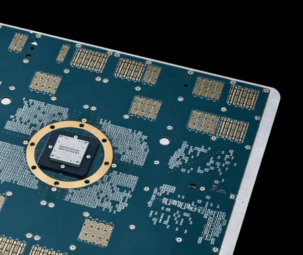
Wafer-Level Test Interface Authority
20μm Precision.
Total Integrity.
Merging 30 years of HDD contact rigor with advanced probing architectures. We define the physical standards for zero-drift electrical contact.
30 Years
ENGINEERING DNA
20μm Pitch
FABRICATION MASTERY
R² = 1.0
VALIDATION STANDARD
Core Division 01
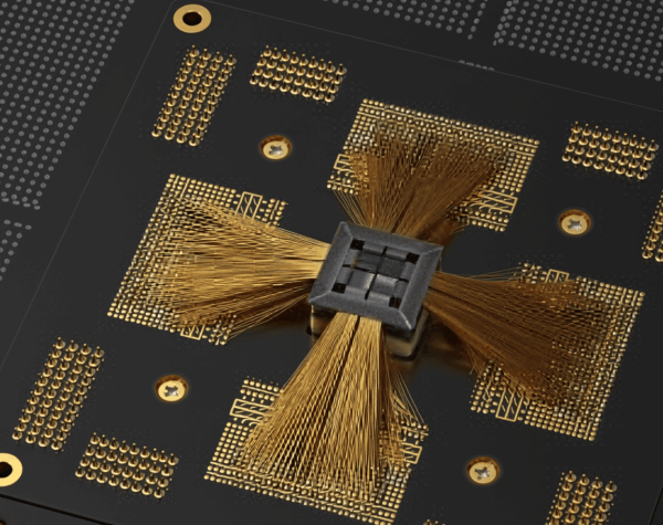
Cantilever Probing.
Specializing in high-pin count DDI, Logic, and Flash Memory nodes. Featuring 20μm staggered pitch resolution and proprietary WRe (750 Hv) metallurgy for extended lifecycle reliability.
- ✔ 6,000+ PIN Capacity
- ✔ Low Leakage Performance (pA level)
- ✔ Rapid 48-hour Maintenance Cycle
Core Division 02
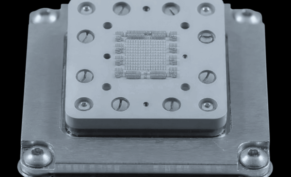
Vertical & MEMS Arrays.
Engineered for 5nm/3nm Advanced Nodes. Our vertical solutions feature zero-scrub vertical integrity to protect delicate Micro-Bumps and Cu-Pillars under high-frequency test cycles.
Max Voltage: <3500V
Probe Material: N7 Alloy / Pd Alloy
Yield Recovery & Maintenance.
Every interface eventually deviates. Galaxy Tech provides sub-micron realignment and planarity tuning using Agilent-verified metrology to minimize your test floor downtime.