Dynamic Interconnect Engineering
High-Performance
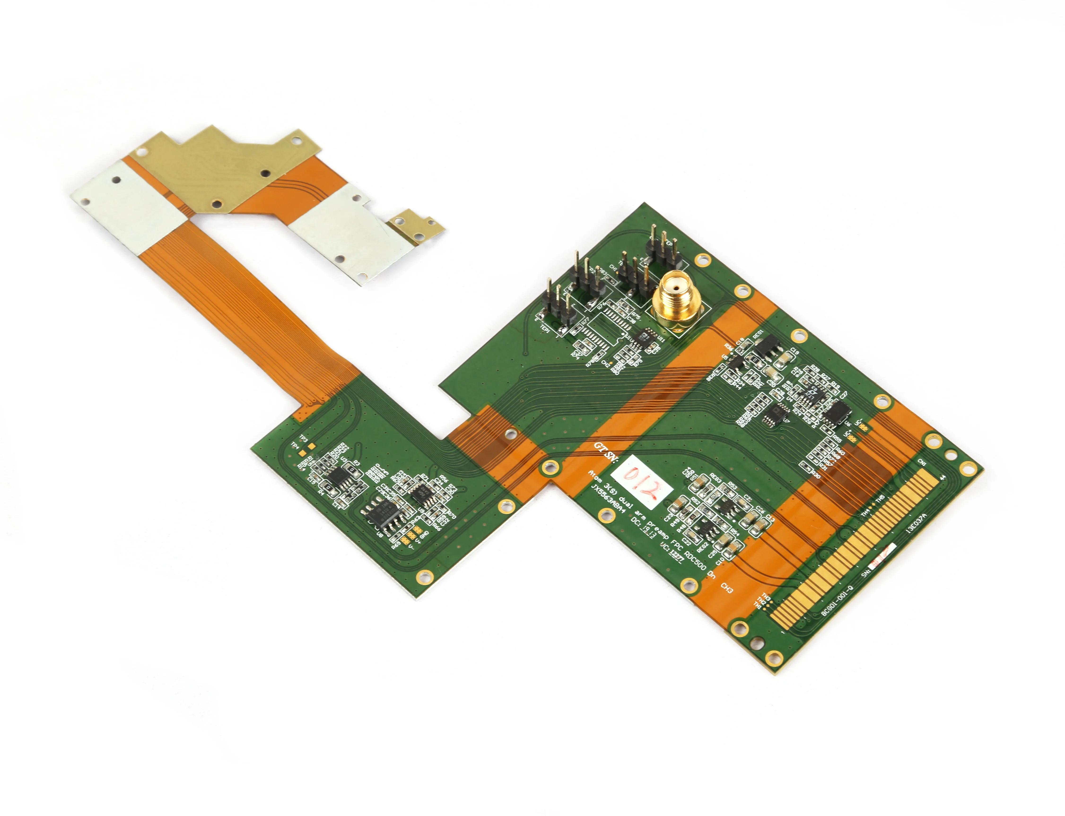
Flexible FPC.
Merging 30 years of HDD-standard dynamic flex rigor with sub-micron fabrication. We deliver multi-layer FPC solutions designed for extreme bending environments and high-frequency signal paths.
1 – 8 LayersFlex Fabrication
±10%Impedance Control
450mmMax Interface Length
Bespoke Solutions
Dynamic Bending
Optimization.
Every FPC is a study in material fatigue and signal integrity. Leveraging our legacy in HDD Slider Dynamic Testing (SDT), we engineer flexible interconnects that withstand millions of cycles without trace fracture or signal degradation.
Validated for High-RPM Simulation & Wafer-Sort Nodes.
FPC Engineering Specification
Precision Fabrication
Min Trace/Space2 / 2 mil
Layer Count1 – 8 Layers
Max Board Size450 x 250 mm
Material Science
Base MaterialPolyimide (PI), PET
Copper Thickness12μm – 70μm
Cover-layPI, Photo-imageable
Surface Finish
Gold PlatingENIG, Hard Gold (50u”)
Solder MaskFlexible Green, Black
StiffenerFR4, SUS, PI