Exacting Build-to-Print Precision
From Slider
To Silicon.
Your blueprints, our engineering rigor. Merging 22 years of HDD dynamic contact heritage with semiconductor-grade interconnect fabrication.
Primary Business
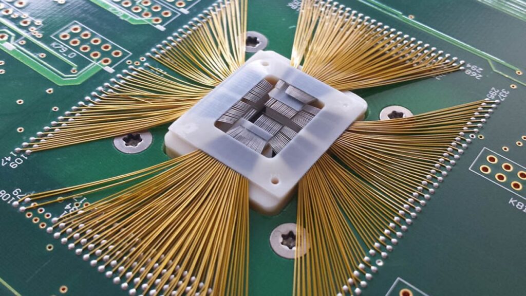
Advanced Probe
Card Fabrication.
Specializing in high-density Cantilever and Vertical Probing architectures. We translate your test site blueprints into high-fidelity hardware, supporting 20μm staggered pitch and up to 6,000+ PIN counts.
WRe (750 Hv) & Pd Alloy Metallurgy | LCD Driver (2.5Gbps) Specialists
Integrated Manufacturing
High-Complexity
Carrier Assembly.
Galaxy Tech manages the assembly of 32-layer rigid-flex carrier boards with ±0.03mm placement precision. Optimized for Flip-Chip and high-lead-count BGA characterization.

Yield Engineering
Data-Backed
Quality Verification.
Build-to-print execution is verified by Automated X-Ray Metrology and Active Calibration. We provide the mathematical proof (R² = 1.0) that our output matches your design intent.
100% Process Traceability | Agilent-Driven Validation

Integrated Global Network.
Strategic HQ
Hong Kong
Strategic Logistics & IP Oversight.
Technical Liaison
Japan
Advanced Material Sourcing & JDM Liaison.
Manufacturing
Dongguan
Agile Precision Workshop (ISO 9001).