
Wafer-Level Test Interface Authority
20μm Precision.
Total Integrity.
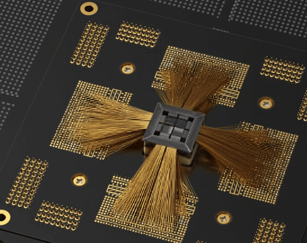
Merging 30 years of HDD contact rigor with advanced probing architectures. We define the physical standards for zero-drift electrical contact in high-density wafer testing.
20μm Pitch
MIN STAGGERED RESOLUTION
6,000+ PINS
MULTI-SITE CAPACITY
WRe / N7
ADVANCED METALLURGY
Display Driver Domain
Exacting LCD/OLED Test Interfaces.
Derived from three decades of mastering micro-contact for HDD preamps. Our cantilever solutions are specifically tuned for high-RPM simulation environments and ultra-fine pad sorting, achieving < 1pA @ 10V leakage performance.
FREQUENCY: UP TO 2.5 Gbps
ALIGNMENT: ± 3.0μm
Process Sovereignty
Automated Probe Geometry Verification.
Execution is verified by physics. Utilizing high-resolution Automated Optical Metrology, we conduct 100% batch validation of probe tip position, alignment, and planarity. Our verification logs ensure that every manufactured interface perfectly matches your design parameters.
- ✔ 100% Automated Tip Position Analysis
- ✔ Planarity Tuning for Multi-Site Consistency
- ✔ Full Dimensional Traceability Reports
